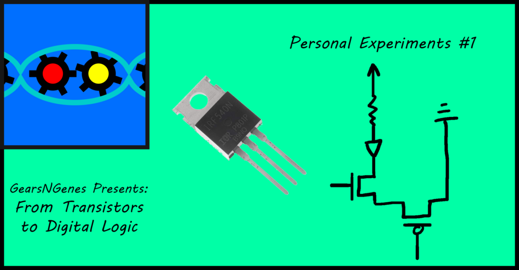
Transistor Experiments #1
Many educational sources describe how to use transistors as switches in circuits, which provides the foundation of digital logic. However, many of these sources lacked a concrete example to demonstrate and explore with. For such a key concept in computing, I decided I would democratize this subject by providing my own demonstrations, which inspired me to create the Transistors and Digital Logic Course.
This post and its series is meant to give a glimpse into my personal learning and investigating process while I developed the course. Additionally, this is to act as a supplementary guide for those seeking to learn more about transistors and digital logic.
After learning that transistors could be used as switches, I decided I would attempt to use the concept to develop an AND gate.
As a brief introduction, an AND gate is a device that takes voltages from two distinct sources and outputs a HIGH voltage if and only if both of the input sources are HIGH as well. If either of them are LOW, then the output voltage is LOW.
A truth table of an AND gate
in1|in2|out
0 | 0| 0
0 | 1| 0
1 | 1| 1
1 | 0| 0
This first experiment is my first attempt at making an AND gate using only N-Channel MOSFET transistors.
N-MOSFETs are devices that, as mentioned before, can act similar to switches. Specifically, if its gate (analogous to our AND’s input voltages) is connected to ground (0 V, indicated as a 0 in digital logic), then it acts as open or disconnected circuits. However, if an N-MOSFET’s gate is connected to a power source (voltage >> 0 V, indicated as a 1 in digital logic), then it acts as closed circuits.
Therefore, to create an AND gate, I needed to connect two N-MOSFETs in series, as seen below:

I then connected an LED between the power source and the first transistor. The inputs of this AND gate are marked by A and B in the image above. When I fed the logic values of the truth table into A and B, I got the expected displays. The LED only lit up on a (1,1), while remaining off for any other ordered pair of values.
Therefore, I succeeded in making an AND, right?
WRONG!
I then discovered that although the LED does light up like it is in an AND gate, it is not a TRUE logic gate.
This is something I did not see discussed once in any of the sources I looked at for the course. The trouble is as follows:
When either of the transistors remain as an open circuit, current doesn’t flow at all through the LED (as expected). However, for a true AND gate, when either of the input voltages are 0, the gate should OUTPUT a 0 V. However, with this circuit, when either sites A or B are 0, the circuit is not closed at all. It is by definition, open. Therefore, it cannot output a 0. Instead, the circuit is in what is known as a “hanging state”.
My next step is to design an AND gate that not just displays like an AND gate but also outputs a VOLTAGE like an AND gate. I will be keeping you all updated.
Until then, stay creative!
